
 English
 usheenthermal

Measured Rebound, Verified Contact: How to Select SHEEN Boron Nitride Thermal Pads
Date:2026-10-15
In server power supplies, power conversion modules, and semiconductor test equipment, the gap between a component and its heat sink is influenced by component height, manufacturing tolerances, surface flatness, and assembly methods. Thermal engineers must select a material that fills this gap under an acceptable mechanical load, establishes effective thermal contact, and meets electrical insulation requirements.
Compressibility determines how well a material accommodates a gap during assembly, while rebound indicates how much of its compressed thickness it recovers after the load is removed. Both properties become important selection criteria when clamping conditions or interface gaps may change.
At SHEEN, we recommend evaluating rebound, thermal resistance, electrical insulation, and assembly load together rather than treating any single specification as the deciding factor. The SF1600-BN Series test data provides a practical starting point for evaluating these properties under defined conditions.[1]
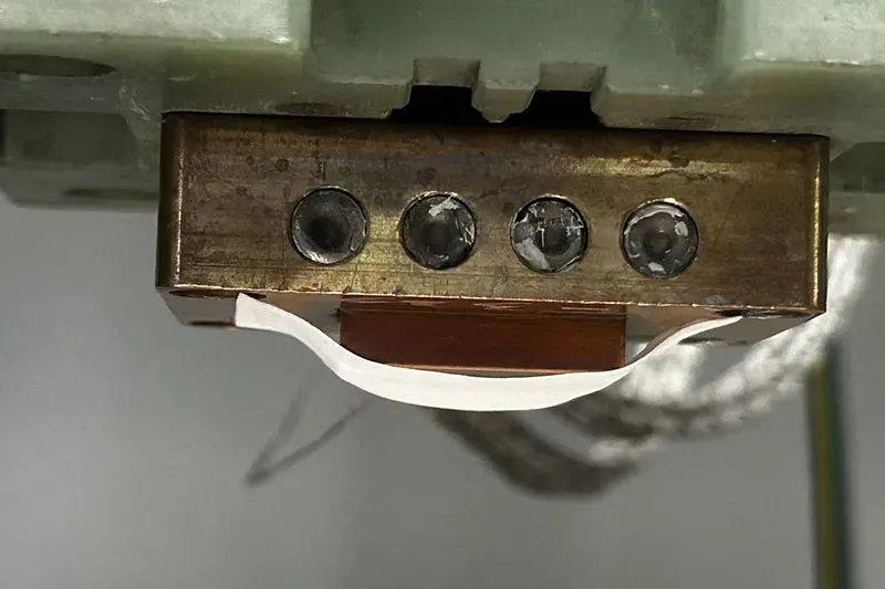
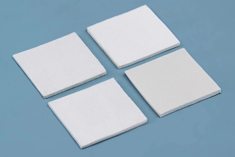
| Test instruments | Condition of the boron nitride thermal pad before testing | Condition of the boron nitride thermal pad after testing |
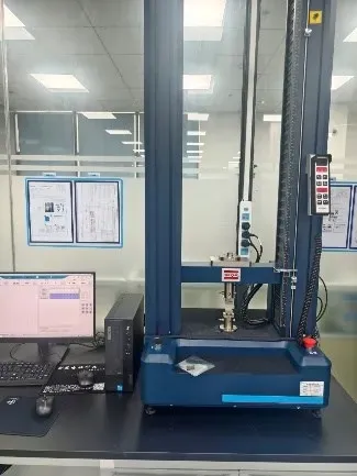 | 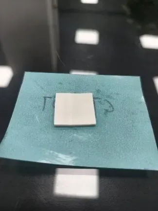 | 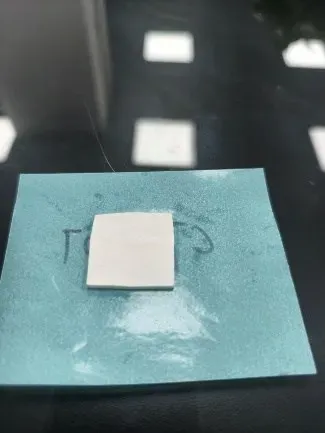 |
Figure 1. Compression test equipment and sample images before and after testing, as documented in the SHEEN test report.[1]
1. A 92% Average Rebound Rate: Measured Evidence of Thickness Recovery
For a thermal interface material that must accommodate changes in an interface gap, one of the first questions is how much thickness it can recover after compression.
The test report evaluated 25 mm × 25 mm × 0.3 mm samples. Each sample was compressed to 50% strain at a rate of 0.5 mm/min and held in the compressed state for 30 minutes. After unloading, the samples were allowed to recover for 10 minutes before their recovered thicknesses were measured. The results for three samples are shown below.[1]
| Test item | Sample 1 | Sample 2 | Sample 3 | Average |
|---|---|---|---|---|
| Rebound rate | 93% | 91% | 92% | 92% |
These results indicate that the 0.3 mm sample recovered most of the thickness lost during compression under the specified test conditions. For engineers assessing post-assembly thickness recovery or a material's ability to accommodate changes in interface gaps, this is a useful performance indicator to investigate through further sample testing.
The report calculates the rebound rate as the recovered thickness divided by the thickness lost during compression.
For example, assume an initial thickness of 0.300 mm and a compressed thickness of 0.150 mm. At a rebound rate of 92%, the sample would recover approximately 0.138 mm, giving a calculated recovered thickness of 0.288 mm, or approximately 96% of its initial thickness.[1]
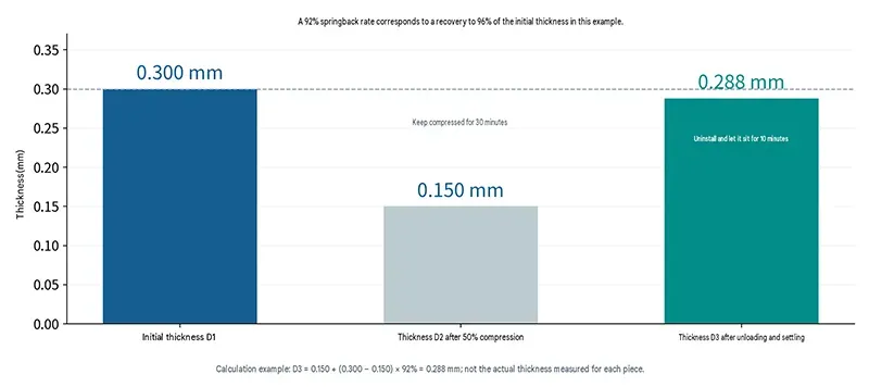
Figure 2. The 0.288 mm recovered thickness is a calculated example based on the nominal thickness and a 92% rebound rate, not an individually measured result. Formula: (D3 − D2) / (D1 − D2) × 100%.[1]
For materials using oriented boron nitride structures, the value of the structure must ultimately be demonstrated through the finished product's mechanical and recovery performance. The SF1600-BN Series uses hexagonal boron nitride as the thermally conductive filler and silicone rubber as the matrix. The test results provide direct evidence of thickness recovery for the thin sample evaluated.[1–2]
2. Thermal Contact Must Be Evaluated Through Interface Thermal Resistance
Thickness recovery helps engineers assess a material's potential to accommodate changes in an interface gap. However, thermal design also requires verification of interface thermal resistance at the relevant pressure and temperature.
The SHEEN report used the ASTM D5470 method to evaluate thermal performance at 80°C and 40 psi. The thermal conductivity obtained by fitting measurements across multiple thicknesses was 16.1 W/(m·K). The independently measured thermal resistance results are summarized below.[1]
| Nominal thickness (mm) | Measured initial thickness (mm) | Measured compressed thickness (mm) | Thermal resistance range for three samples (°C·cm²/W) | Reported average thermal resistance (°C·cm²/W) |
|---|---|---|---|---|
| 0.3 | 0.301–0.303 | 0.260–0.266 | 0.278–0.294 | 0.286 |
| 1.0 | 1.00–1.01 | 0.949–0.950 | 0.691–0.698 | 0.695 |
| 1.5 | 1.50–1.51 | 1.306–1.310 | 0.968–0.980 | 0.974 |
At 80°C and 40 psi, the 0.3 mm sample achieved an average thermal resistance of 0.286 °C·cm²/W. This result is consistent with the specification of ≤0.3 °C·cm²/W listed in the SF1600-BN-03 datasheet.[1–2]
Based on the average thickness measurements in the report, the sample was compressed from 0.302 mm to 0.264 mm, representing approximately 12.6% thickness reduction. This finding highlights the importance of evaluating a thermal pad under realistic assembly pressure and gap conditions. A larger compression value observed during testing should not automatically be treated as the design target.
For interfaces with tight gaps, clear electrical insulation requirements, and limited thermal resistance budgets, the SF1600-BN-03 is worth including in a sample evaluation. Other thickness options can be considered when the interface gap requires a thicker material.
3. Seven Thickness Options for Matching Thermal and Electrical Requirements
The seven SF1600-BN models share a nominal thermal conductivity of 16 W/(m·K), with nominal thicknesses ranging from 0.3 mm to 3.0 mm. Their rebound, thermal resistance, and AC breakdown voltage specifications are listed below.[2–8]
| Model | Nominal thickness (mm) | Rebound specification | Thermal resistance specification (°C·cm²/W) | Thermal resistance test pressure | AC breakdown voltage specification (kV) |
|---|---|---|---|---|---|
| SF1600-BN-03 | 0.3 | ≥90% | ≤0.3 | 40 psi | ≥4 |
| SF1600-BN-05 | 0.5 | ≥80% | ≤0.5 | 40 psi | ≥5 |
| SF1600-BN-07 | 0.7 | ≥70% | ≤0.7 | 40 psi | ≥6 |
| SF1600-BN-10 | 1.0 | ≥70% | ≤0.8 | 40 psi | ≥10 |
| SF1600-BN-15 | 1.5 | ≥60% | ≤1.1 | 40 psi | ≥12 |
| SF1600-BN-20 | 2.0 | ≥60% | ≤1.4 | 40 psi | ≥12 |
| SF1600-BN-30 | 3.0 | ≥60% | ≤1.7 | 30 psi | ≥12 |
Note: Values are compiled from the respective model datasheets. The SF1600-BN-30 thermal resistance specification is based on a test pressure of 30 psi, while the other six models specify 40 psi. Their thermal resistance values should therefore not be treated as a direct comparison at an identical pressure.[2–8]
All seven models also specify a volume resistivity of ≥10¹³ Ω·cm, a relative dielectric constant of ≤4.2 at 1 MHz, and a UL 94 V-0 flammability rating.[2–8]
A practical selection process starts with the actual interface gap, followed by a review of thermal resistance and insulation specifications. The final step is to validate assembly load and thermal contact using physical samples.
Where the material can reliably fill the gap while meeting insulation and mechanical load requirements, engineers can assess whether a thinner model is suitable and then verify its thermal resistance under actual assembly conditions.
4. A Practical Gap Example: How to Screen Candidate Samples
Consider an electrically insulating thermal interface with an assembled gap of 1.6–1.8 mm. An engineer wants to begin the evaluation with a 2.0 mm thermal pad.
For this simplified calculation, thickness tolerances are ignored. A 2.0 mm pad compressed into a 1.8 mm gap experiences 10% compression, while the same pad in a 1.6 mm gap experiences 20% compression.
The compression stress data for the 2 mm sample in the SHEEN report can provide an initial reference for assessing whether the resulting mechanical load warrants further evaluation. The test sample measured 25 mm × 25 mm × 2 mm and was compressed at a rate of 0.5 mm/min.[1]
| Compression strain | Sample 1 instantaneous stress (psi) | Sample 2 instantaneous stress (psi) | Sample 3 instantaneous stress (psi) | Reported average stress (psi) |
|---|---|---|---|---|
| 10% | 21.80 | 17.65 | 16.35 | 18.60 |
| 20% | 38.51 | 34.12 | 31.28 | 34.63 |
| 30% | 69.42 | 60.32 | 54.36 | 61.36 |
| 40% | 101.14 | 89.35 | 78.24 | 89.57 |
| 50% | 168.26 | 150.37 | 142.35 | 153.66 |
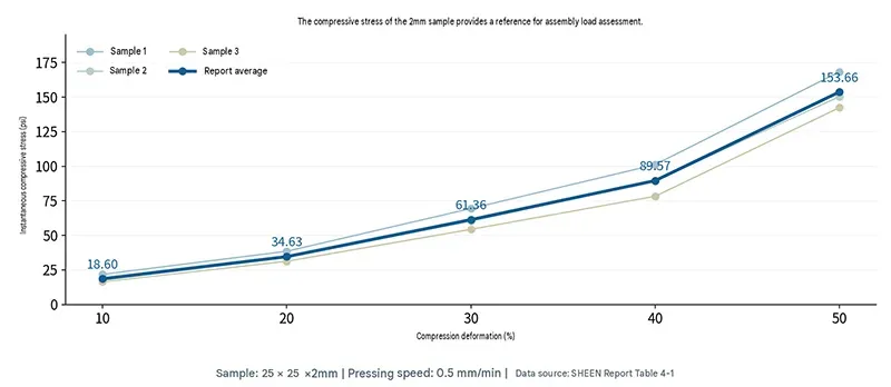
Figure 3. Compression Stress Testing of 2mm Boron Nitride Thermal Pads.[1]
In this example, the average instantaneous stress was 18.60 psi at 10% compression and 34.63 psi at 20% compression. Engineers can use these values as an initial reference, together with component load limits, effective contact area, and the mechanical design of the clamping structure, to decide whether to proceed with sample testing.
The next steps are to confirm thickness tolerances, measure the actual installed condition, and verify thermal resistance and electrical performance at the intended pressure and deformation.
The SF1600-BN-20 datasheet specifies thermal resistance of ≤1.4 °C·cm²/W at 40 psi. That specification should not be directly assigned to this example, which considers 10–20% compression without establishing that the corresponding interface pressure is 40 psi.[7]
The screening process is straightforward: determine the gap, calculate the required compression, use the compression stress data as a preliminary load reference, and then validate thermal performance using actual samples.
5. Which Engineering Projects Should Consider Sample Evaluation?
AI Server Power Supplies and Power Conversion Modules
When electrical insulation is required and component height tolerances affect the gap between a device and its heat sink, engineers can screen candidate models based on the minimum and maximum gap and the allowable component load.
Key validation items include compressed thickness, temperature rise, and electrical insulation performance.
Semiconductor Test Equipment
Where thermal contact mechanisms involve changes in clamping conditions, the rebound data from the 0.3 mm sample can serve as an initial screening reference.
For applications involving frequent opening and closing or repeated reuse, sample testing should cover the intended number of cycles and monitor changes in recovered thickness, thermal resistance, and electrical insulation.
Photovoltaic Inverters and Energy Storage Power Conversion Systems (PCS)
For electrically insulating thermal interfaces in power electronics, candidate thicknesses can be selected according to the minimum and maximum interface gaps. Performance should then be verified under the actual clamping arrangement and operating temperature.
These applications are suitable candidates for targeted evaluation. Whenever possible, use samples with dimensions, surface conditions, and clamping arrangements representative of the final design. This helps ensure that test results are useful for subsequent engineering decisions.
6. Understanding Test Conditions and Planning Sample Validation
The rebound, thermal resistance, and compression stress values discussed in this article come from different tests. The 92% average rebound rate is a measured result for the 0.3 mm sample under the stated test conditions. For other thicknesses, refer to the specifications in their respective datasheets and confirm the rebound test procedures during material selection.[1–8]
The report also shows that the 2 mm sample had an average instantaneous stress of 153.66 psi at 50% compression. After the compression was maintained for 600 seconds, the average residual stress was 34.40 psi, indicating stress relaxation under sustained deformation.[1]
Assembly design should therefore consider both the initial load and whether sufficient contact pressure will remain over time. These data alone, however, do not establish that thermal contact will remain unchanged throughout long-term service.
After 1,000 hours of aging at 125°C, the 1.5 mm sample showed a 14.2% increase in thermal resistance relative to its initial value. The report does not provide post-aging rebound results or repeated-compression lifetime data.[1]
For applications involving low clamping loads, repeated assembly and disassembly, or long-term operation, sample validation should include thermal resistance at the actual operating pressure, recovery over the intended compression cycles, and thermal and electrical performance after aging.
Breakdown voltage is a material test result obtained under specified conditions. System-level insulation design must also account for the compressed thickness, operating voltage, and applicable requirements.[2–8]
7. Request Evaluation Samples Matched to Your Interface Conditions
If your project requires thermal conductivity, electrical insulation, and the ability to accommodate an interface gap, Contact SHEEN to discuss material selection and sample evaluation for the SF1600-BN Series.
To make the initial technical discussion more efficient, we recommend providing four types of information:
- Interface geometry: Minimum and maximum gap, along with the proposed thermal pad dimensions.
- Thermal requirements: Component type, power dissipation, operating temperature, and target temperature rise, where available.
- Mechanical and electrical requirements: Insulation requirements, available clamping pressure, and allowable component load.
- Operating conditions: Repeated clamping, disassembly, thermal cycling, or other special service conditions.
If some parameters have not yet been finalized, you can start by sharing an assembly drawing or photos of the component and heat sink, together with a description of the current temperature rise, contact, or insulation challenge.
When requesting samples, mention “SF1600-BN Material Selection Evaluation” and request the datasheets and relevant test conditions for the candidate models. Sample thickness, dimensions, quantity, and delivery arrangements can be confirmed during the discussion.
Start with a shortlist of technically justified candidates, then validate their performance in your actual interface. The measured rebound results, thermal resistance data, and model-specific insulation specifications of the SHEEN SF1600-BN Series provide a clear starting point for that process.
Product and technical information: www.sheenthermal.com
Technical Datasheet information: www.sheenmaterials.com
References
[1] SHEEN, SF1600-BN Series Boron Nitride Thermal Pad Performance Test Report. Compression stress and residual stress after 600 seconds: p. 6; rebound test method and results: pp. 7–8; thermal resistance: pp. 4–5; high-temperature aging: p. 17. Measured results represent only the samples and conditions described in the report. Calculated values are identified separately.
[2] SF1600-BN-03 Datasheet.
[3] SF1600-BN-05 Datasheet.
[4] SF1600-BN-07 Datasheet.
[5] SF1600-BN-10 Datasheet.
[6] SF1600-BN-15 Datasheet.
[7] SF1600-BN-20 Datasheet.
[8] SF1600-BN-30 Datasheet.
Sheen Thermal
Dongguan Sheen Electronic Technology Co., Ltd · Founded in 2008
Manufacturer of thermal interface materials and silicone foam for automotive electronics, energy storage, power electronics, communications and consumer electronics.
Certified
- ISO 9001:2015
- ISO 14001:2015
- IATF 16949:2016
What we supply
- Thermal conductivity Up to 90 W/m·K
- Thickness 0.3–10.0 mm
- Custom & samples Die-cut to drawing, 3–7 days
LAST:Nothing