
 English
 usheenthermal

Too Hard and It Won’t Conform, Too Soft and It Won’t Install: The R&D Tightrope of Boron Nitride Thermal Pads
Date:2026-10-24
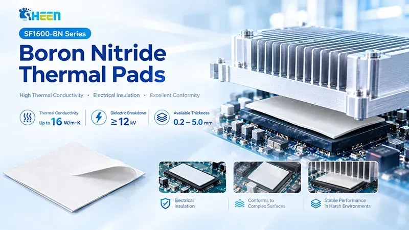
A thermal pad sitting between a power device and its heatsink has three jobs at once: move heat out, provide electrical isolation, and survive assembly. Sheen’s SF1600-BN series uses boron nitride as the thermally conductive filler in a silicone rubber matrix — a thermal interface family built around the combined demands of heat transfer, insulation, and surface conformity, with selectable thicknesses for power, telecom, and smart-device applications.
The Hard Part of R&D: Everything Trades Off Against Everything
Making a high-quality, cost-effective BN thermal pad is not just a conductivity arms race. Here’s the tug-of-war we live with in development:
- BN material needs enough mechanical strength to survive die-cutting, liner peeling, handling, and assembly.
- But strengthen the material, and hardness creeps up — conformability drops, and contact thermal resistance climbs with it.
- Soften it instead, and yes, it fills micro-gaps beautifully… until it tears, stretches out of shape, or becomes a handling nightmare on the line.
That’s why we insist on a combined evaluation when selecting materials, never a single-number beauty contest. Under near-1D heat flow, total interface resistance is the sum of bulk resistance and contact resistance on both sides. Conductivity governs how well heat moves through the material; actual thickness, contact pressure, and surface condition decide whether that ability shows up in your device.
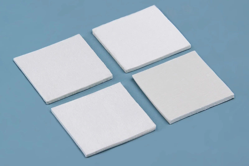
Figure 1 — SF1600-BN Thermal Pad Series Product Overview
Sheen’s development direction for BN materials goes beyond conductivity — we keep pushing processability and handling so samples glide into customer trial builds instead of dying on the bench. Judging a pad means looking at its thermal resistance under a defined pressure, and at whether it stays in one piece through peeling, transfer, and installation.
Make the Material Fit the Process, Not the Other Way Around
The value of a BN pad also lives in its formulation and processing headroom. Our current BN pad range covers 0.2–5.0 mm thickness, and we can confirm thickness, tolerance, outline, and packaging around your project. Custom-spec thermal resistance and insulation values should be re-verified on the actual samples — paper agreements don’t conduct heat.
One of our R&D goals is simply: behave yourself in standard die-cutting and assembly. Less scrap from tearing, warping, or positioning headaches. That means you can evaluate liner-peel integrity, die-cut edge quality, and installation efficiency in the same round as thermal performance — which is where they belong.
- Hardness: Shore C 60–80 — but judge conformability from the compression curve, not the durometer alone.
- Recovery rate is not a stand-in for tensile or tear strength. Different properties, different tests.
- Compliance: the SF1600 series meets RoHS 2.0, halogen-free, and REACH requirements — usable as evidence in your material compliance review.
Commercial BN fillers now come in many forms and specs, which gives formulation work a solid raw-material base. For procurement teams, the long-term value of a BN pad also hinges on lot-to-lot consistency, processing yield, and delivery capability. Cost the material by thickness, size, and usage — comparing per-piece prices while ignoring assembly scrap and validation cost is how budgets quietly bleed out.
How Assembly Pressure Moves Resistance and Compression
Look at the SF1600-BN-03 curve below. Across the tested range, raising pressure lowers thermal resistance and raises compression — no surprises, but the magnitude matters. At 40 psi, thermal resistance is ≤0.30 °C·cm²/W and compression ≥15%.
The takeaway: a pad must be evaluated together with its assembly pressure, and the actual design still has to respect the device’s pressure limits. The material can take it doesn’t mean the package can.
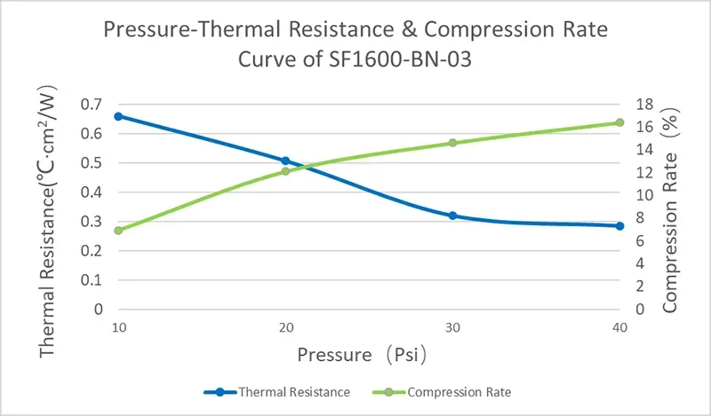
Figure 2 — SF1600-BN-03 (0.3 mm) pressure vs. thermal resistance & compression rate curve
Interfaces That Need Isolation: Confirm the Insulation Spec First
In power conversion, PV inverters, and anywhere live devices meet metal cooling structures, electrical isolation is a system-level design issue. For these interfaces, thermal performance only counts after insulation requirements are met. Hexagonal boron nitride conducts heat while insulating electrically — which is exactly why it’s such a valuable filler for insulating thermal composites.
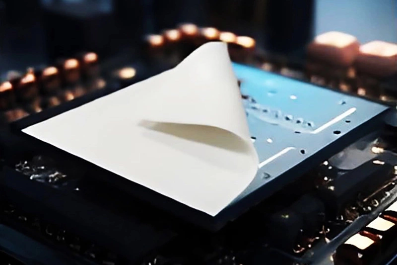
Our belief at Sheen: as power density keeps climbing, materials that carry heat and isolation in one layer will keep finding work. But — and this matters — check breakdown voltage, compressed thickness, and the use environment during selection. A material’s breakdown voltage is not your device’s long-term operating voltage. Don’t size your safety margin off a lab coupon.
Semiconductor test, telecom equipment, intelligent-driving electronics, and humanoid robots all have different structures — yet all of them can surface heat-dissipation interfaces that demand electrical isolation. One BN material platform can offer candidates for each; then it’s temperature, gap, and electrical conditions, verified case by case.
Three Thicknesses, Head to Head
SF1600-BN-03, -10, and -20 share the same 16 W/m·K conductivity. What changes with thickness is thermal resistance, AC breakdown voltage, and recovery rate — enough to narrow your sample validation list before you cut parts.
| Item | SF1600-BN-03 | SF1600-BN-10 | SF1600-BN-20 |
|---|---|---|---|
| Thickness | 0.3 mm | 1.0 mm | 2.0 mm |
| Thermal conductivity | 16 W/m·K | 16 W/m·K | 16 W/m·K |
| Thermal resistance @ 40 psi | ≤0.30 °C·cm²/W | ≤0.80 °C·cm²/W | ≤1.40 °C·cm²/W |
| AC breakdown voltage | ≥4 kV | ≥10 kV | ≥12 kV |
| Recovery rate | ≥90% | ≥70% | ≥60% |
Common parameters: operating temperature −40 to 150 °C; density 1.6 ± 0.2 g/cm³; volume resistivity ≥10¹³ Ω·cm (250 V); dielectric constant ≤4.2 (1 MHz); flame rating UL94 V-0. Thermal resistance per ASTM D5470; AC breakdown voltage per ASTM D149. Listed resistance values are area-normalized results under stated test conditions — not standalone contact resistance, and not system-level resistance. Recovery rates as listed in the datasheet.
Pick Thickness from the Real Gap
SF1600-BN-03 at 0.3 mm suits small gaps with good flatness and tight tolerance control. It carries the lowest nominal resistance of the three — a first look for compact power devices, test equipment, and thin thermally conductive joints that need insulation.
SF1600-BN-10 at 1.0 mm balances gap-filling and heat transfer, with AC breakdown ≥10 kV — a candidate for AI server power supplies, telecom power, and power control board interfaces.
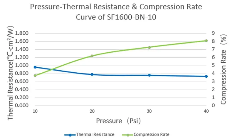
Figure 3 — SF1600-BN-10 (1.0 mm) pressure vs. thermal resistance & compression rate curve
Reading Figure 3: resistance drops as pressure rises, then flattens; compression keeps climbing. When selecting, work from the device’s allowable pressure and confirm what assembly conditions your target resistance actually requires.
SF1600-BN-20 at 2.0 mm covers structures that need to bridge larger assembly gaps, with AC breakdown ≥12 kV. For power modules, energy-storage PCS, or robot control equipment, sample it against your structural tolerances. All of the above are selection directions — final say belongs to system-level validation.
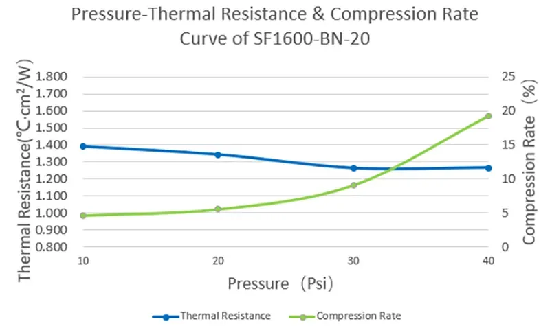
Figure 4 — SF1600-BN-20 (2.0 mm) pressure vs. thermal resistance & compression rate curve
One curve worth a second look: in Figure 4, resistance falls, then ticks slightly upward at the end of the test range while compression keeps rising. More pressure does not guarantee ever-lower resistance — the exact cause needs the raw data and repeat testing, not armchair extrapolation.
Thickness selection should cover the gap tolerance and land at a sensible compression. Blindly going thicker stretches the heat path; blindly going thinner risks insufficient contact. Within the bounds of reliable gap-filling, insulation, and pressure limits — evaluate the thinner option first.
Prove the Choice in Real Conditions
【Request a Custom Quote】For BN thermal pads, what Sheen cares about is whether the material works stably once it’s inside your device. During sample validation, record thermal resistance or device temperature rise, compression, assembly integrity, and insulation performance before and after aging — so lab parameters line up with real use conditions.
If your project is looking for an interface material that handles both heat transfer and insulation, send our team your minimum and maximum gap, heat source size, allowable pressure, operating temperature, and withstand-voltage requirement. Ask for SF1600-BN-03, -10, or -20 samples with their matching documentation — and start the validation from thickness screening.
Sheen Thermal
Dongguan Sheen Electronic Technology Co., Ltd · Founded in 2008
Manufacturer of thermal interface materials and silicone foam for automotive electronics, energy storage, power electronics, communications and consumer electronics.
Certified
- ISO 9001:2015
- ISO 14001:2015
- IATF 16949:2016
What we supply
- Thermal conductivity Up to 90 W/m·K
- Thickness 0.3–10.0 mm
- Custom & samples Die-cut to drawing, 3–7 days
LAST:Nothing