
 English
 usheenthermal

Advancing PV Inverter Reliability via Boron Nitride Thermal Pad Heat Dissipation
Date:2026-07-17
Advancing PV Inverter Reliability via Boron Nitride Thermal Pad Heat Dissipation
Boron Nitride Thermal Pad Heat dissipation for photovoltaic inverters is no longer a niche upgrade — it is the line between steady output and costly shutdowns as heat quietly strangles modern power modules.
Grease pumps out, graphite risks shorts, and phase materials age fast; downtime and warranty claims pile up quicker than expected.
In 2025, Sheen Technology engineers emphasize insulation and consistency as key to inverter longevity.
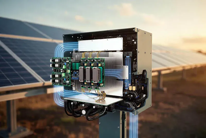
Key Insights: Boron Nitride Thermal Pad Heat dissipation for photovoltaic inverters
· Superior Conductivity: Lowers junction temperatures in IGBT and MOSFET modules, preventing thermal runaway and boosting inverter efficiency.
· Electrical Insulation: High dielectric strength safeguards DC-AC converter circuits under high-voltage conditions.
· Conformable Interface: Optimal compressibility ensures intimate contact across uneven surfaces, minimizing thermal impedance.
· Long-Term Stability: Maintains performance over wide temperature ranges, reduces thermal cycling stress, and extends device lifetime.
Why Thermal Management Matters for PV Inverters
PV inverters face a unique set of thermal challenges that distinguish them from other power electronics applications:
· Daily thermal cycling: Inverter operation follows the solar diurnal cycle, producing repeated thermal ramps from cool morning startup to peak-load midday heat and back to nighttime cooldown. This cycling accelerates TIM degradation mechanisms such as grease migration and bond-line fatigue.
· High ambient temperatures: Rooftop and ground-mount inverters operate in enclosures exposed to direct sunlight, with internal ambient temperatures reaching 70–85 °C. The delta between ambient and junction temperature is compressed, demanding lower thermal resistance at every interface.
· Long service life requirements: Commercial PV installations target 20–25 year operational lifespans. The TIM must maintain its thermal and electrical performance over this entire period without maintenance or replacement.
· High-voltage isolation: String inverters operate at 600–1500 V DC input, requiring the TIM to provide reliable electrical isolation between the power module baseplate and the grounded heat sink throughout the operating life.
BN thermal pads address each of these requirements through a silicone-BN composite that remains electrically insulating, thermally conductive, and mechanically stable across the full PV inverter operating envelope.
5 Key Benefits Of BN Thermal Pads In PV Inverters
For PV inverter power stages operating under continuous cycling and high-voltage bias, BN thermal pads deliver five engineering advantages that directly impact system reliability.
Benefit 1. Enhanced Thermal Conductivity for Lower Junction Temperature
Core effect:
· Thermal conductivity boosts heat transfer
· Lowers junction temperature
· Stabilizes power electronics in PV inverters
Practical chain:
· Heat leaves chip fast
· Heat dissipation improves
· Runaway risk drops
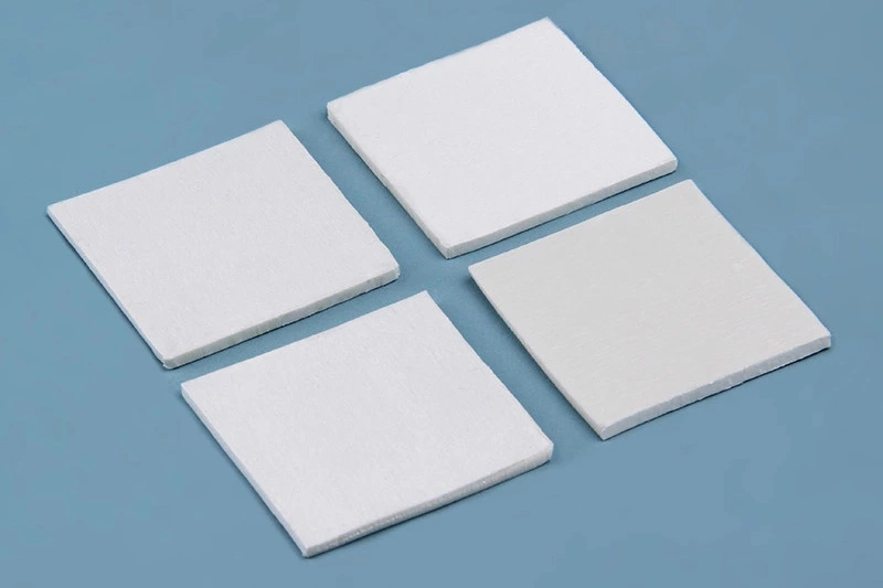
| Properties | Unit | SF1600-BN-sp-03(0.3mm) | Test Method |
| Color | - | White | Visual |
| Thermal Conductivity | W/m·K | 16 | ASTM D5470 |
| Thermal Resistance (@40psi) | ℃*cm2/W | ≤0.3 | ASTM D5470 |
| Application temperature | ℃ | -40~150 | - |
| Thermal weight loss rate | % | ≤1 | - |
| Thickness | mm | 0.2~5.0 | ASTM D374 |
| Breakdown voltage | KV,@AC | ≥4 | ASTM D149 |
| Dielectric constant | F/m, @ 1MHz | ≤4.2 | ASTM D150 |
| Volume resistivity | Ω*cm, @250V | ≥1013 | ASTM D257 |
| Rebound rate | % | ≥90 | - |
| Density | g/cm³ | 1.6±0.2 | ASTM D792 |
| Hardness | shore 00 | 60~80 | ASTM D2240 |
| Flammability rating | - | V-0 | UL 94 |
Boron Nitride Thermal Pad: Heat dissipation for photovoltaic inverters keeps silicon happier under load. With boron nitride, heat spreads evenly, not in hotspots.
Benefit 2. Superior Electrical Insulation & Dielectric Strength
Protection stack: BN thermal pads provide dielectric strength exceeding 4 kV AC at 0.3 mm thickness, with volume resistivity above 10¹³ Ω·cm. This ensures reliable isolation between the DC bus (600–1500 V) and the grounded heat sink across the 20+ year inverter service life.
Application layer:
· Power modules — maintain isolation — improve safety
Short version: strong insulation plus cooling in one pad. That's why BN thermal pads fit tight DC-AC designs.
Benefit 3. Optimal Compressibility for Superior Conformability
Contact mechanics: BN thermal pads achieve 20–40% deflection at typical mounting pressures (10–50 psi), allowing them to conform to surface irregularities of Ra 0.8–3.2 µm. This eliminates the air gaps that would otherwise add 0.2–0.5 °C·cm²/W of interfacial thermal resistance.
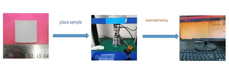
Sheen Technology laboratory Boron Nitride Thermal Pad Compressive stress test:
· Sample preparation: Material dimensions of 25mm x 25mm x 2mm.
· Test method
1) Zero the force reading before testing; apply a 2N force to make contact with the sample surface.
2) For the compressive stress test, set the compression speed to 0.5 mm/min and the deformation range to 10–50%. For the residual stress test, set the compression speed to 0.5 mm/min and the hold time to 600 seconds.
| Test Item | Test Data | |||||
| Sample | 10% | 20% | 30% | 40% | 50% | |
| Instantaneous stress (psi) at 10–50% deformation | 1 | 21.80 | 38.51 | 69.42 | 101.14 | 168.26 |
| 2 | 17.65 | 34.12 | 60.32 | 89.35 | 150.37 | |
| 3 | 16.35 | 31.28 | 54.36 | 78.24 | 142.35 | |
| Average Value | 18.60 | 34.63 | 61.36 | 89.57 | 153.66 | |
| Residual compressive stress at 50% deformation | Sample | 1 | 2 | 3 | Average Value | |
| 40.61 | 34.96 | 27.62 | 34.40 | |||
Multi-step view: press → conform → spread heat. A well-fitted pad quietly upgrades Boron Nitride Thermal Pad Heat dissipation for photovoltaic inverters.
Benefit 4. Wide Operating Temperature Range Stability
Environment handling: BN pads maintain stable thermal and electrical performance across –40 °C to +150 °C, covering the full range of PV inverter operating conditions from cold desert mornings to peak-load rooftop temperatures.
Reliability loop:
· Steady thermal stability
· Survives temperature cycling
Across deserts or rooftops in winter, performance stays consistent. No sudden drops in thermal performance.
Benefit 5. Improved Long-Term Device Lifetime
Aging control: By reducing junction temperature and eliminating TIM degradation mechanisms, BN pads directly extend the mean time between failures (MTBF) of IGBT and MOSFET modules. The Arrhenius relationship predicts that every 10 °C reduction in junction temperature doubles the semiconductor device lifetime.
Outcome:
· Fewer component failure events
· Longer device lifetime
Multiple short takeaways: cooler chips last longer. Stable pads mean fewer surprises. Boron Nitride Thermal Pad Heat dissipation for photovoltaic inverters directly supports long-term reliability in every PV inverter.
Sheen Technology provides detailed technical datasheets for BN thermal pads designed specifically for PV inverter power stages. Download the PV Inverter Series Datasheet for complete engineering specifications, including recommended pad thickness by inverter power class, clamping torque guidelines, and thermal simulation support files.
Materials Layering for Heat Dissipation in PV Inverters
Effective thermal management in a PV inverter requires optimizing the entire heat path from semiconductor junction to ambient air. BN thermal pads play a central role in three distinct layers of this path.
Interface Layer: BN Filler in Polymer Matrix
The pad-to-module interface is where heat transfer is made or broken. The BN filler network within the silicone matrix provides a thermal conductivity of 16 W/mK in the through-plane direction, while the silicone matrix conforms to surface micro-geometry.
Key design parameters: BN loading ratio (typically 60–80% by weight), particle size distribution (bimodal for optimal packing density), and filler alignment (press-direction orientation maximizes through-plane conductivity). Sheen Technology controls all three parameters at the compounding stage to ensure batch-to-batch consistency.
Intermediate Layer: Conformable Die-Cut Thermal Pad
The BN pad itself serves as a mechanical buffer between the rigid module baseplate and the heat sink surface. Its compressibility accommodates flatness tolerances (typically 50–100 µm), component tilt, and thermal expansion mismatch without transferring excessive stress to solder joints.
Process chain: The pad is die-cut to match the module footprint, placed on the baseplate, compressed during heat sink mounting, and verified for final thickness. Sheen Technology offers pads from 0.5 mm to 5.0 mm thickness with ±0.1 mm tolerance.
Heat Sink Coupling: Enhancing Transfer to the Cooling System
The final layer connects the pad to the fin-stack or cold plate. Coupling quality depends on three factors: contact pressure (target 200–300 kPa), surface flatness (target <50 µm across the mounting area), and torque pattern (cross-tightening to 70% of final torque, then final pass to 100%).
When all three layers are optimized, the total thermal resistance from junction to ambient is minimized, and the BN pad delivers its full rated performance. Sheen Technology provides application-specific mounting recommendations for common PV inverter heat sink designs.
Diagnosing and Preventing Thermal Runaway in PV Inverters
Even with proper TIM selection, installation quality determines real-world performance. The following diagnostic and integration practices help engineers identify and eliminate thermal risks.
Reducing Thermal Impedance at Power Modules
Where losses hide:
· Air gaps in power modules
· Poor interface materials
· Inconsistent mounting pressure
Interface optimization
· Pad selection — thickness vs thermal resistance
Contact quality
· Void reduction
· Pressure balance
Boron Nitride Thermal Pad: Heat dissipation for photovoltaic inverters cuts heat transfer loss noticeably. Sheen Technology pads are tuned for tight interface bonding.
Optimizing Heat Flux in IGBT and MOSFET Arrays
Common imbalance signs:
· Overworked IGBT
· Cooler adjacent MOSFET zones
Deep layout tuning:
· Heat path alignment — center vs edge loading
· Flux balancing — pad conductivity uniformity
Boron Nitride Thermal Pad Heat dissipation for photovoltaic inverters keeps heat flux even, avoiding localized burnout. Sheen Technology solutions help stabilize array behavior.
Surface Preparation for Reliable Pad Bonding
Prep checklist:
· Degrease surfaces
· Smooth micro-roughness
· Verify flatness
Surface preparation
· Cleaning quality
Thermal interface materials bonding
· Adhesion strength
· Air gap elimination
Boron Nitride Thermal Pad: Heat dissipation for photovoltaic inverters depends on clean contact more than fancy specs. Done right, it locks in long-term manufacturing process stability.
Sheen Technology BN thermal pads are deployed across a wide range of PV inverter platforms. Visit the applications for application notes, reference designs, and case studies showing how BN pads are specified across different power classes, voltage ratings, and thermal budgets in real-world PV installations.
Can BN Thermal Pads Extend Inverter Lifespan?
The short answer is yes, through three mechanisms: thermal cycling resistance, sustained power density, and reduced aging rate.
Evaluating Thermal Cycling Resistance Improvements
Core idea: Thermal cycling hits hard when temperature fluctuations repeat daily in PV inverters.
Interface behavior
· Boron nitride fillers keep thermal pads dimensionally steady
· Lower resistance drift maintains contact
Mechanical impact
· Reduced micro-cracks → higher reliability
· Longer lifespan under cycling loads
Practical takeaway
· Consistent Boron Nitride Thermal Pad Heat dissipation for photovoltaic inverters = fewer reworks
Small note: Sheen Technology tunes pad elasticity to absorb expansion without losing pressure, so interfaces stay tight.
Impact on Power Density and Efficiency Over Time
Short take: cooler junctions = happier silicon.
| Metric | No BN pad | BN pad | Long-run effect |
|---|---|---|---|
| Power density | Medium | Higher | Sustained output |
| Efficiency | Drops | Stable | Less degradation |
| Performance | Fluctuates | Steady | Longer operational life |
· Using boron nitride thermal pads, heat spreads fast; PV inverters hold efficiency curves flatter.
· Repeat it in real ops: Boron Nitride Thermal Pad Heat dissipation for photovoltaic inverters keeps conversion tight even on hot afternoons.
Minimizing Thermal Resistance to Prevent Device Aging
Steps that actually matter:
1) Cut interface gaps — lower thermal resistance
2) Improve heat transfer paths across sinks
3) Keep chips below stress thresholds — slower device aging
Quick hits:
· Less component degradation, more uptime
· Stable reliability in dusty, hot arrays
· Consistent Boron Nitride Thermal Pad Heat dissipation for photovoltaic inverters avoids hotspot creep
Sheen Technology solutions focus on thin, uniform pads that don't pump out, keeping contact solid year after year.
For thermal engineers designing or upgrading PV inverter platforms, BN thermal pads from Sheen Technology provide the documented performance, batch consistency, and application support needed to achieve 20+ year inverter reliability targets.
Contact our thermal engineering team for a technical datasheet, free sample kit, or application-specific thermal simulation support. Sheen Technology provides BN thermal pads in thicknesses from 0.5 mm to 5.0 mm, with custom die-cutting and adhesive backing options for high-volume production.
Sheen Technology — Thermal Interface Materials for the Next Generation of Power Electronics.
| TIM Type | Thermal Conductivity | Key Strength | Key Limitation |
|---|---|---|---|
| BN Thermal Pad | 16 W/mK | Electrical isolation + thermal path in one layer | Fixed thickness; conformability depends on compressibility |
| Carbon Fiber Thermal Pad | 15–45 W/mK | High compression, high resilience. | The interfacial thermal resistance is relatively high. |
| Graphene Thermal Pad | 75–90 W/mK | Though-plane, low thermal resistance | Requires reflow; risk of bleed-out |
Sheen Thermal
Dongguan Sheen Electronic Technology Co., Ltd · Founded in 2008
Manufacturer of thermal interface materials and silicone foam for automotive electronics, energy storage, power electronics, communications and consumer electronics.
Certified
- ISO 9001:2015
- ISO 14001:2015
- IATF 16949:2016
What we supply
- Thermal conductivity Up to 90 W/m·K
- Thickness 0.3–10.0 mm
- Custom & samples Die-cut to drawing, 3–7 days