
 English
 usheenthermal

How to Select a Boron Nitride Thermal Pad for SiC/GaN Power Modules
Date:2026-07-17
How to Select a Boron Nitride Thermal Pad for SiC/GaN Power Modules
Boron Nitride Thermal Pad Heat dissipation for IGBT, SiC/GaN power modules is where overheating stops killing performance and margins, plain and simple.
Old interface materials slide, dry out, or short your confidence on the line.
IDTechEx and Yole Group report rising demand for insulating pads.
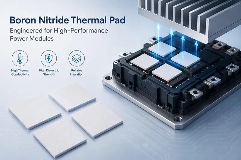
Harmonic Key Points: Boron Nitride Thermal Pad Heat dissipation for IGBT, SiC/GaN power modules
· High Thermal Conductivity: Rapidly lowers junction temperature in SiC MOSFETs and GaN HEMTs, boosting efficiency under heavy heat flux.
· Dielectric Strength: Ensures safe high-voltage isolation in EV inverters and industrial drives, safeguarding module reliability.
· Installation Precision: Clean surfaces, align pads to die attach, and apply even pressure to eliminate air pockets and maintain consistent heat transfer.
Types Of Thermal Interface Materials
Getting heat out of power devices isn't just nice — it keeps everything alive and stable. From Boron Nitride thermal pad heat dissipation for IGBT to SiC/GaN power modules, each material plays its own role. Pick smart, or performance drops fast.
Boron Nitride Pad
Core idea: thermal conductivity meets electrical insulation in one clean layer
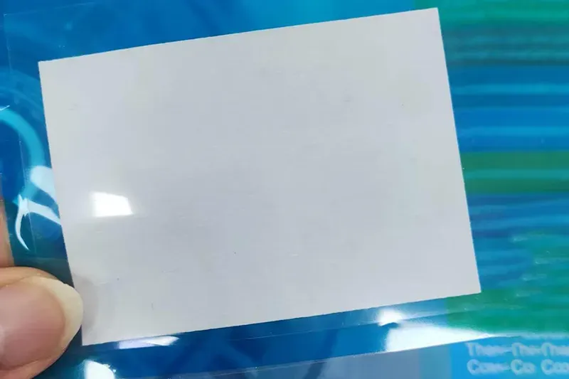
Use cases
· IGBT modules
· SiC/GaN power modules
· High dielectric strength setups
Why engineers keep choosing it
· Handles high temperature without drift
· Good compressibility, fills micro gaps
· Safe, non-toxic handling
Short notes:
Boron Nitride Thermal Pad: Heat dissipation for IGBT stays stable under load. For SiC/GaN heat dissipation, it avoids leakage risks. Sheen Technology pushes consistent pad thickness, which matters more than people expect.
Thermal Grease
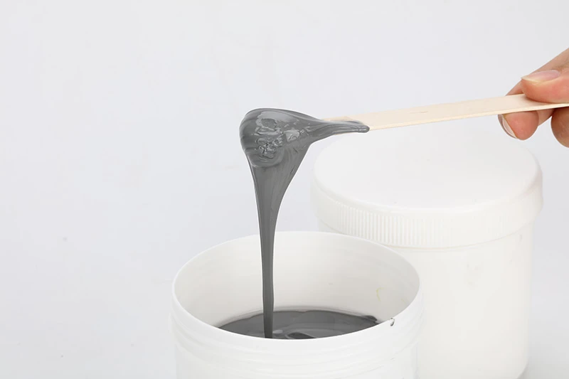
Performance path
· Spread thin → create thin bond line
· Fill voids → reduce air pockets
· Stabilize → resist pump-out
Types
· silicone-based for flexibility
· non-silicone for cleaner environments
Quick hits:
Low viscosity helps flow, but too low gets messy. Thermal paste works best when application method is controlled.
Phase Change Material
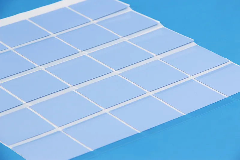
Behavior chain
· Solid → reaches melt temperature
· turns semi-liquid
· boosts wetting
Benefits
· Improved thermal cycling reliability
· Controlled film thickness
Simple take: it adapts when heat rises, tightening contact without extra pressure.
Gap Filler
Problem → uneven surfaces
Solution
· soft pad with conformability
· fills gaps using compressibility
Key traits
· absorbs vibration
· reduces thermal resistance
· easy dispensing
Used a lot where tolerances aren't perfect. Sheen Technology gap fillers stay stable even after long cycling.
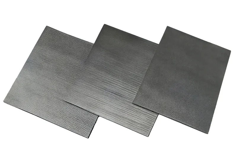
Graphite Sheet
Structure insight
· anisotropic conductivity:spreads heat sideways fast
Advantages
· ultra thinness
· flexibility and lightweight build
Watch-out
· needs an electrical isolation layer
In compact systems, graphite quietly moves heat away before hotspots even form.
5 Key Criteria To Choose Boron Nitride Thermal Pad Heat Dissipation For SiC/GaN Power Modules
When specifying a BN thermal pad for wide-bandgap power modules, engineers should evaluate the following five criteria in sequence.
High Thermal Conductivity: Rapid Heat Flux Reduction
Core requirement: The pad must extract heat faster than the die generates it. For SiC/GaN modules operating above 200 W/cm², the TIM should deliver bulk thermal conductivity of at least 5 W/mK, with correspondingly low thermal impedance (<0.5 °C·cm²/W at target mounting pressure).
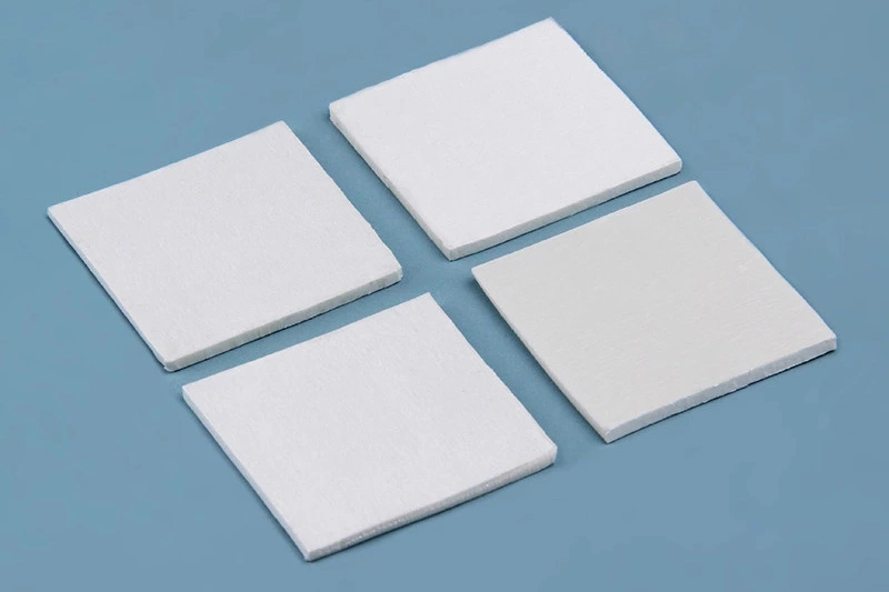
Sheen Technology Boron Nitride Thermal pad performance properties:
| Properties | Unit | SF1600-BN-sp-03(0.3mm) | Test Method |
| Color | - | White | Visual |
| Thermal Conductivity | W/m·K | 16 | ASTM D5470 |
| Thermal Resistance (@40psi) | ℃*cm2/W | ≤0.3 | ASTM D5470 |
| Application temperature | ℃ | -40~150 | - |
| Thermal weight loss rate | % | ≤1 | - |
| Thickness | mm | 0.2~5.0 | ASTM D374 |
| Breakdown voltage | KV,@AC | ≥4 | ASTM D149 |
| Dielectric constant | F/m, @ 1MHz | ≤4.2 | ASTM D150 |
| Volume resistivity | Ω*cm, @250V | ≥1013 | ASTM D257 |
| Rebound rate | % | ≥90 | - |
| Density | g/cm³ | 1.6±0.2 | ASTM D792 |
| Hardness | shore 00 | 60~80 | ASTM D2240 |
| Flammability rating | - | V-0 | UL 94 |
Practical impact: A BN pad with 16 W/mK conductivity reduces junction temperature by 10–15 °C compared to standard fiberglass-reinforced pads at equivalent thickness. This directly improves switching efficiency and extends device lifetime.
In thermal interface material design for power modules:
· High conductivity filler → faster heat transfer
· Reduced junction temp → stable switching
Better Boron Nitride Thermal Pad Heat dissipation for IGBT, SiC/GaN power modules
Dielectric Strength for High-Voltage Isolation
Core requirement: SiC/GaN modules operate at DC bus voltages of 400–800 V (automotive) or 1200 V (industrial). The BN pad must maintain dielectric strength exceeding 4 kV AC at the specified thickness, with volume resistivity above 10¹³ Ω·cm.
Practical impact: In a traction inverter, the pad sits between the module baseplate (at bus potential) and the grounded heat sink. A BN pad with adequate dielectric strength prevents partial discharge and ensures safe operation through the device lifetime without adding a separate isolation film.
Application layers:
· SiC power modules
· GaN power modules
A solid Boron Nitride Thermal Pad Heat dissipation for IGBT, SiC/GaN power modules setup balances insulation and cooling without trade-offs.
Bond Line Thickness Optimization
Core requirement: The pad thickness must be thin enough to minimize thermal impedance but thick enough to accommodate surface roughness, component tilt, and mounting pressure variations.
Optimization guidelines:
· Target thickness: 0.5–2.0 mm depending on gap tolerance
· Compression range: 20–40% deflection at rated clamping force (typically 30–70 psi)
· Surface roughness compensation: pad must conform to Ra 0.8–3.2 µm surfaces
Sheen Technology provides BN pads in calibrated thickness increments to allow fine-tuning without custom tooling.
Surface Wettability with Silicone Elastomer
Core requirement: The pad surface must wet the mating surfaces adequately to minimize interfacial air gaps. BN pads achieve this through the inherent conformability of the silicone matrix combined with the platelet structure of BN fillers.
Step flow:
· Silicone matrix spreads under moderate pressure, conforming to surface asperities
· Air gaps shrink from >40% of interface area (dry contact) to <5% (with BN pad)
· Thermal contact resistance drops correspondingly
Sheen Technology pad formulations are optimized to balance conformability with dimensional stability — soft enough to wet surfaces, firm enough to resist extrusion under clamping load.
Curing Profile Impact on Reliability Testing
Core requirement: For pre-cured pad formats, the manufacturing cure profile determines long-term stability. Fully cured silicone-BN composites resist post-cure shrinkage, outgassing, and thermal aging.
Performance checkpoints:
· Thermal cycling: <3% change in thermal impedance after 2,000 cycles (–40 °C to +150 °C)
· Power cycling: stable contact resistance through 10,000+ power cycles
· Aging: <0.1% weight loss at 125 °C (no volatile fractions)
Sheen Technology BN pads undergo full cure validation per batch, ensuring that the material properties specified on the datasheet are maintained over the application lifetime.
Sheen Technology provides detailed technical datasheets for BN thermal pads designed specifically for SiC/GaN power modules. Download the Technical Datasheet for complete engineering specifications, including recommended pad thickness by module type, clamping torque guidelines, and thermal simulation support files.
Installation Best Practices for BN Thermal Pads
Proper installation is essential to realizing the datasheet performance of BN thermal pads. The following three practices address the most common failure modes in SiC/GaN power module assembly.
Prep Surfaces: Cleaning Substrate and Baseplate
A clean interface is the foundation of low thermal resistance. Even microscopic contamination adds measurable thermal impedance.
Recommended cleaning procedure:
· Inspect both the module baseplate and heat sink mounting surface for residue, oxidation, or machining debris
· Clean with isopropyl alcohol (99%+ purity) using lint-free wipes; change wipes frequently to avoid redepositing contaminants
· Verify cleanliness: surface should appear dry and streak-free under angled lighting
· Apply the BN pad within 30 minutes of cleaning to minimize recontamination
Sheen Technology recommends repeating wipe cycles on high-power builds using boron nitride pad stacks.
Align Boron Nitride Pad to Die Attach Layer
Misalignment redirects heat flow away from the active die area, reducing effective thermal performance by 15–30% in severe cases.
Alignment procedure:
· Center the BN pad over the die attach footprint; the pad should extend 1–2 mm beyond the die edges on all sides
· For multi-die modules (e.g., six-pack IGBT + diode stages), use a single pad covering the full baseplate or individual pads per die position based on assembly preference
· Lightly tack the pad in place at one corner; micro-adjust before applying full pressure
Sheen Technology offers custom die-cut BN pads pre-sized to specific module footprints, reducing alignment variability in production.
Prevent Air Entrapment under the Silicone Pad
Trapped air at the interface can increase local thermal resistance by 2–5x, creating hotspots that accelerate device failure.
Installation sequence:
· Initial contact: lower the heat sink onto the pad from one edge, allowing air to escape from the opposite side
· Pressure application: apply clamping force gradually and evenly — use a torque wrench with a cross-tightening pattern
· Final set: after reaching target torque, allow 5–10 minutes for pad compression to stabilize before power-on
Sheen Technology recommends slow, progressive compression passes to keep the BN pad interface void-free, particularly in large-format SiC modules where air entrapment risk is highest.
Comparison of Thermal Interface Materials for Power Modules
| TIM Type | Thermal Conductivity | Key Strength | Key Limitation |
|---|---|---|---|
| BN Thermal Pad | 16 W/mK | Electrical isolation + thermal path in one layer | Fixed thickness; conformability depends on compressibility |
| Thermal Grease | 1–5 W/mK | Thin bond line, low cost | Pump-out, dry-out, migration risk |
| Phase Change Material | 3–8 W/mK | Melts to fill gaps, low thermal resistance | Requires reflow; risk of bleed-out |
| Silicone Gap Filler Pad | 1–15 W/mK | Fills large uneven gaps, vibration damping | Higher thermal resistance at thin bond lines |
| Graphene Sheet | 75-90 W/mK (though-plane) | Very high though-plane spreading | Requires separate electrical isolation layer |
Page support:
· Visit the applications page for application notes, reference designs, and case studies showing how BN pads are specified across different power levels, voltage classes, and thermal budgets.
· Request a Technical Datasheet or Engineering Sample. Sheen Technology provides BN thermal pads in thicknesses from 0.5 mm to 5.0 mm, with custom die-cutting and adhesive backing options for high-volume production. Contact our thermal engineering team for a technical datasheet, free sample kit, or application-specific thermal simulation support.
Sheen Thermal
Dongguan Sheen Electronic Technology Co., Ltd · Founded in 2008
Manufacturer of thermal interface materials and silicone foam for automotive electronics, energy storage, power electronics, communications and consumer electronics.
Certified
- ISO 9001:2015
- ISO 14001:2015
- IATF 16949:2016
What we supply
- Thermal conductivity Up to 90 W/m·K
- Thickness 0.3–10.0 mm
- Custom & samples Die-cut to drawing, 3–7 days