
 English
 usheenthermal

Thermal Pad Selection for GPU-Accelerated Computing: An Engineering Guide for AI Servers, Edge Inference & Industrial GPU Modules
Date:2026-08-06
GPU-accelerated computing modules — from data center AI training accelerators (NVIDIA H100/B200, AMD MI300X) to edge inference processors and industrial visualization GPUs — now routinely operate at 300–700W TDP. Unlike single-die CPUs where thermal grease or liquid metal suffices, GPU modules present a multi-component cooling challenge: the GPU die, HBM memory stacks (or GDDR modules), and voltage regulator (VRM) stages each require precisely specified thermal interface materials (TIMs).
Thermal pads are the dominant TIM choice for GPU memory and VRM interfaces because they accommodate height variation across multiple components, provide electrical isolation, and maintain consistent bond-line thickness (BLT) over the product lifecycle. This engineering guide covers the key parameters for GPU thermal pad specification, compares material options, and provides integration guidance for OEM assembly and system integration.
Thermal pads are robust elastomeric materials engineered to:
- Fill microscopic voids between uneven surfaces;
- Maintain uniform contact pressure;
- Deliver high thermal conductivity and excellent electrical insulation.
- Selecting the appropriate thermal pad not only enhances cooling efficiency but also ensures long-term stability, reduces fan noise, and extends the GPU's lifespan.
Key Parameters for Selecting GPU Thermal Pads
Choosing the right thermal pad isn't just about picking the one with the highest thermal conductivity or the most expensive option. It requires balancing multiple characteristics based on the GPU's specifications and the thermal pad's parameters.Let's delve into the key parameters:
Thermal Pad Thickness
The most common mistake when replacing a GPU thermal pad is using an improper thickness. An excessively thick pad may prevent full contact between the heatsink and component, reducing cooling efficiency. Conversely, a pad that is too thin may fail to fully cover the gap, leading to air pockets that increase thermal resistance. Therefore, Conduct gap analysis using pressure-sensitive film or laser profilometry across multiple GPU module samples to establish mean gap and ±3σ tolerance. Specify pad thickness based on the compression ratio target (typically 15–30% of original thickness) at the assembly clamping pressure.
For production environments, pad thickness tolerance should be specified as ±5% of nominal. Sheen Technology provides thickness-controlled pads with in-line laser measurement verification.
Thermal Conductivity (W/m·K)
Measured in W/m·K, thermal conductivity indicates a material's inherent heat transfer capability. Entry-level pads rated at 3–6 W/m·K suit mainstream GPUs, while 8–12 W/m·K pads suit GPUs with higher-end memory. Premium pads offer even higher thermal conductivities of 12–20+ W/m·K. However, higher conductivity isn't always better—it increases cost and alters hardness and density, potentially compromising perfect contact in practice. Selecting pads with appropriate thermal conductivity is therefore crucial.
Thermal conductivity should be evaluated per ASTM D5470 (steady-state) at the target BLT and clamping pressure. Through-plane conductivity values reported without test conditions (pressure, thickness) are not directly comparable across suppliers.
For GPU memory (GDDR/HBM) thermal management, through-plane conductivity of 6–10 W/m·K is typically sufficient when combined with proper BLT control (<200 μm). Higher conductivity (12–20 W/m·K) may be justified for direct GPU die interfaces using phase-change or gel TIMs.
Flexibility and Compressibility
The flexibility and compressibility of thermal pads are typically measured by Shore hardness values, indicating how easily the pad compresses. Soft, highly compressible thermal pads better conform to uneven surfaces like GPU memory or MOSFET areas. Harder pads may resist compression, creating excessive gaps and potentially damaging delicate components under excessive pressure.
Sheen Technology's SP Series thermal phase-change materials remain solid at room temperature for easy assembly and handling. Upon reaching the phase-change temperature, they thermally soften into a liquid state with excellent wettability, effectively filling gaps between heat sinks and electronic components.

Dielectric Strength and Electrical Insulation
Selecting non-conductive, insulating thermal pads is essential, particularly when handling sensitive GPU components, to prevent short circuits. For instance, Graphene sheet thermal pads offer excellent thermal conductivity but are electrically conductive, potentially causing graphics card short circuits.
Sheen Technology's boron nitride-filled thermal pads combine high thermal conductivity, superior insulation, and high resilience, making them an ideal choice for GPUs.
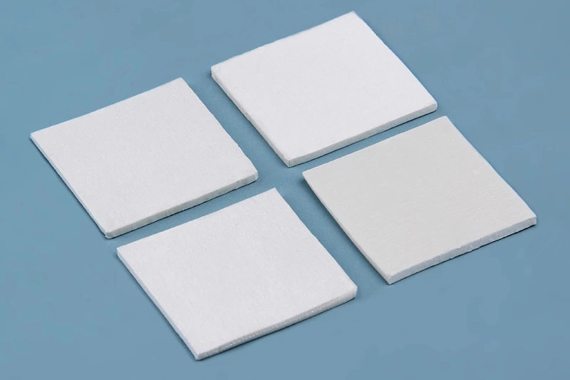
Sheen Technology Recommended GPU Thermal Pad Materials and Installation Techniques
| Material Type | Thermal Conductivity | Electrical Properties | Typical Applications |
| Silicone-based pad | 1–15 W/m·K | Insulating | GDDR memory, VRM stages |
| Boron Nitride (BN) pad | 16 W/m·K | Insulating | HBM stacks, high-power VRM |
| Phase-Change (PCM) | 3–8 W/m·K | Insulating | GPU die (TIM1/TIM2) |
| Graphene pad | 75–90 W/m·K | Conductive | Thermal spreaders, ultra-thin gaps |
| Test Method | ASTM D5470 | - | - |
OEM Assembly Integration: Thermal Pad Installation Best Practices
1.Incoming Material Specification and Verification
- Verify pad thickness, hardness, and visual quality on incoming inspection per the material specification sheet
- Conduct first-article inspection (FAI) for die-cut pad dimensions using optical measurement
- Perform thermal conductivity spot-check on witness samples using ASTM D5470 or equivalent
- Archive lot numbers for full batch traceability to raw material certificates
2.Substrate Preparation for Production Assembly
- Specify surface cleanliness: free of flux residue, finger oils, and particulates per IPC-A-610 Class 2/3
- Automated plasma or vapor-degreasing stations recommended for volume >1,000 units/day
- Post-cleaning surface energy verification: ≥40 dynes/cm using contact-angle measurement or dyne pens
3.Pad Placement and Assembly
- Pre-cut pads supplied in tape-and-reel or tray format for SMT pick-and-place compatibility
- Automated placement using vision-aligned pick-and-place systems (tolerance: ±0.1 mm)
- Cross-pattern screw tightening sequence with calibrated torque drivers (typically 4–8 kgf·cm for GPU modules)
- Inline thickness or pressure verification after assembly; log data for SPC trending
4.Post-Assembly Validation
- Thermal validation: measure junction temperature under rated TDP load; compare to thermal model predictions
- First-article thermal impedance testing: verify BLT via cross-section or X-ray on sacrificial samples from each batch
- Production sampling plan: 1–5% of units undergo thermal validation depending on criticality and volume
Request an OEM Assembly Process Consultation →【Sheen Engineering Team】
At Sheen Technology, we understand that effective thermal management is a science. Through research into advanced fillers like boron nitride, we explore formulations that deliver exceptional thermal conductivity without compromising compressibility or long-term stability. We are committed to developing advanced thermal management solutions that integrate materials science with precision engineering.
By correctly matching specific hardware requirements with thermal pads, we significantly enhance product thermal performance and longevity, unlocking the full potential of your hardware.
Sheen Thermal
Dongguan Sheen Electronic Technology Co., Ltd · Founded in 2008
Manufacturer of thermal interface materials and silicone foam for automotive electronics, energy storage, power electronics, communications and consumer electronics.
Certified
- ISO 9001:2015
- ISO 14001:2015
- IATF 16949:2016
What we supply
- Thermal conductivity Up to 90 W/m·K
- Thickness 0.3–10.0 mm
- Custom & samples Die-cut to drawing, 3–7 days